MitySOM-A5E PCIe Gen 3x4 EP Example Project
 This page is a work in progress. When this warning is removed, the instructions should be considered finalized.
Overview
This example demonstrates using the Agilex 5 PCIe Hard IP in an Endpoint (EP) configuration at Gen 3 (8 GT/s) link rates with x4 data lanes. In this example, the end connector interface of the MitySOM-A5E Standard Development Kit is connected to a host PC running linux Ubuntu via a samtec PCIEC-064-0500-EC-EM-P-85 cable assembly.
The demonstration allows a host PC to perform the following tasks:
- Transfer data from a Host PC memory buffer to the HPS SDRAM memory. Data can also be viewed by the HPS processor.
- Transfer Data from the HPS SDRAM memory to a Host PC memory buffer.
- Read the contents of the SYSID module that is in the Agilex 5 FPGA fabric and shared between the Host PCIE access and the lightweight HPS to FPGA bridge.
A block diagram of the example is shown below.
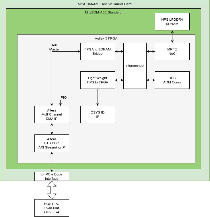
This demonstration does not include support for SDRAM cache coherency management between the Agilex-5 ARM complex and the SDRAM memory. The Agilex-5 ARM accesses the memory using non-cache modes.
The FPGA project utilizes the "Multi-Channel DMA IP for PCIe block" to facilitate transfers from the GTS PCIe EP Streaming IP to the FPGA2SDRAM AXI bridge.
Users should refer to the Multi-Channel DMA IP for PCIe Block Design Example User Guide for information about the HOST software supported by this IP.
Supported Hardware
- MitySOM-A5E Standard Development Kit Baseboard (all variants)
- A5ED-B64-188-SRC-X (default)
- A5ED-B64-144-SRC-X
- A5ED-B66-188-SRC-X
- A5ED-B66-144-SRC-X
Known Issues and Limitations
- No Cache management on the ARM complex is performed in the example
- This example currently does not demonstrate throughput measurements
- This example does not demonstrate the HPS sending MSI IRQs to the HOST for notification of events.
Requirements
- Quartus Prime Pro Edition 25.3.1
- AArch64 cross-compiler toolchain (e.g.,
aarch64-none-linux-gnu-gccoraarch64-linux-gnu-gcc) - Reference SD card with a compatible Linux filesystem
- This project is configured for HPS-first boot
- Ubuntu 24.04.2 Linux PC supporting 64-bit PCIe transfers
- Open PCIe slot with x4 lanes available
- Samtec PCIEC-064-0500-EC-EM-P-85 PCIe Slot to Edge cable extender.
Building the FPGA Design
Follow the instructions for building the fpga and bootloader but use the reference project in the directory named "mitysom-a5e-ref-pcie-gen3x4-ep" in the folder with the desired MitySOM-A5E.
In addition to the FPGA JIC and a5e.core.rbf files, this example requires using the socfpga_agilex5_mitysom_devkit_pcie_ep.dtb device tree file in order to create a HPS 32 MB memory carve-out at 0x882000000 that the HOST PC can safely read and write to without corrupting the linux kernel page tables or memory management. The boot.cmd file in the FPGA project scripts folder (generated with make uboot_script) must be updated to include the carve-out.
Deploy the FPGA firmware
Update the FPGA firmware, kernel devicetree, and boot script files as described in the Deploying the Firmware section of the FPGA Build instructions.
After flashing the JIC file, the last step, power off the board.
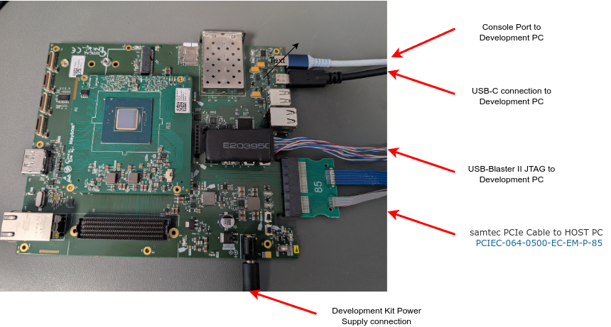
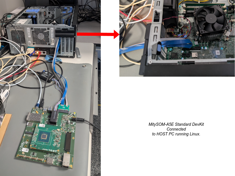
Connecting the Target to the HOST PC
With both the Target MitySOM-A5E development kit and the test HOST PC turned off, assemble the connected system according to the figures below.
Power up the Boards
Note: the MitySOM-A5E carrier card development kit does not use power supplied by the PCIe Edge Connector. It must be powered using the external +12V supply on the barrel connector. In order for the Agilex-5 PCIe EP to properly enumerate on the HOST PC PCIe bus, the MitySOM-A5E carrier card must be powered and the FPGA configured first. After the FPGA has been configured, the HOST PC can be powered on (or restarted) in order for the HOST PC to properly detect the EP device.
To ensure the HOST PC sees the A5E on the PCIe bus, run lspci and look for Unassigned class [ff00]: Altera Corporation Device 0000 (rev 01) in the output.
Copy PC Test Software and Drivers onto HOST PC
The example project folder in the git repository also includes a snapshot of software provided by Altera when the PCIe EP example project is generated. The folder is called "p0_software". Copy the contents of this folder to the HOST PC using:
rsync -rap p0_software user@host_pc:
Build and install the kernel and kernel UIO drivers
Section 3.5.5 of the Altera Multi Channel DMA IP for PCIe Design Example User Guide outlines the necessary steps for compiling the kernel and additional modules needed to support running the PCIe DMA software. For this example, the custom ifc_uio.ko kernel driver is used to facilitate transferring data to the Agilex-5 PCIe EP. Follow the instructions in Section 3.5.7.1.1 for the UIO driver installation.
Build and install the User Space Library
Following the instructions in Section 3.5.7.1.3 of the User Guide to install the libmqdmasoc.so library in the /usr/local/lib folder of the HOST PC operating system.
Build the example applications
Follow the instructions in Section 3.5.7.1.4 to build the perfq_app application program. The perfq_app program can be used to read and write over the PIO (leightweight AXI bus) to read the SYSID value of the QSYS ID core.
A separate application is available for DMA'ing a simple data pattern to the HPS SDRAM. To compile this application:
cd p0_software/user/cli/sample
make clean
make
This will generate a program called "ref" that can be used to transmit a counting pattern into the HPS SDRAM area or read back an HPS SDRAM area to a local buffer.
Run the example application
Quick Check
The following script, located in p0_software/user/cli/perfq_app/load.sh, can be used to setup the hugepages parameter, load the needed uio modules, and read out the SYSID parameter from the PIO proxy bus:
#!/bin/bash
echo 40 | sudo tee /proc/sys/vm/nr_hugepages
sudo modprobe uio
sudo insmod /home/$USER/p0_software/kernel/driver/kmod/mcdma-custom-driver/ifc_uio.ko
lspci -d 1172:000 -v | grep ifc
sudo ./perfq_app -b 0000:03:00.0 -o --pio_r_addr=0x0000 --bar=2
You should see an output similar to this:
40
        Kernel driver in use: ifc_uio
READ: PIO  Address = 0x0         Value = 0x6997296700000001, bar = 2
Where the value should be consistent with the SYSID fields of the quartus project.
Note that the load.sh script in the git repository may required editing to correct paths to the p0_software area.
Transmitting Data to the Agilex-5 HPS SDRAM
On the HOST PC run the command:
cd p0_software/user/cli/sample
sudo ./ref 0x882A00000 tx
On the Agilex-5 HPS console, you can check the contents of the transferred memory by running the following command:
memtool 0x882A00000 32
This will dump out the first 32 4 byte words stored in memory. It should match the counting pattern generated by the ref application.
Reading Data back from the Agilex-5 HPS SDRAM
On the HOST PC run the command:
cd p0_software/user/cli/sample
sudo ./ref 0x882A00000 rx
This should read data back from the same location in the Agilex-5 HPS SDRAM and dump out the contents of the first several words to the display.